
Technical Information
Camera / Product
Proprietary IP Core Technology
"Teli Core Technology"
- Enabling Deterministic Control Beyond Speed -

Machine vision systems require not only high-quality image acquisition but also stable, real-time control. In industrial camera applications, response times for image capture timing and parameter changes have a significant impact on overall system performance and reliability.
Toshiba Teli's proprietary Teli Core Technology is an IP core for industrial cameras that achieves deterministic camera control by implementing time-critical camera control processes as dedicated hardware circuits within an FPGA rather than executing them on a CPU.
In addition to delivering stable response performance with minimal influence from CPU-based control, it provides significantly faster response times than conventional approaches for register access and software-trigger operations.
Why Image Quality Alone Is Not Enough
Industrial cameras are required to deliver more than just high image quality.
In actual inspection equipment and image processing systems, the following are critical:
- Exposure must start precisely when commanded
- Parameter changes must take effect at the intended timing
- System behavior must remain consistent across installations
- Performance must remain stable and reproducible after startup
In other words, what truly matters is:
"Not simply being able to capture images, but being able to capture them the same way every time."
Camera Control Architecture Comparison
Different camera manufacturers employ various architectures for the control section, which serves as the heart of the camera.
The following summarizes two common architectures widely used in industrial cameras and highlights how Teli Core Technology differs from them.
① FPGA + All-in-One Chip Architecture
This architecture performs camera control using a chip that integrates both interface functions and a CPU.
It is cost-effective, highly versatile, and widely adopted in industrial cameras.
Features
- High versatility
- Easy feature expansion through software
- Simple system configuration
Challenges
Since control processing is performed by a CPU, response times may vary depending on:
- CPU load
- OS scheduling
- Communication conditions

② Standard Interface IP + CPU Core Architecture
This architecture incorporates a CPU core inside the FPGA and implements control processing in software.
Its flexibility makes it well suited for feature-rich cameras.
This was also the architecture used in our previous camera models.
Features
- Easy implementation of proprietary features
- Advanced control capabilities
- Effective utilization of FPGA flexibility
Challenges
Because processing relies on a CPU, there are inherent limitations in minimizing:
- Processing latency
- Task contention
- Response-time variation

③ Teli Core Technology
With Teli Core Technology, time-critical control processes are implemented as dedicated hardware circuits inside the FPGA rather than being executed on a CPU.
Features
- CPU-less control
- High-speed response
- Stable response timing
- Deterministic control behavior
Value Delivered
- Stable equipment performance
- Predictable camera response
- Reduced system integration effort
- Improved timing reproducibility
These advantages contribute to enhanced reliability throughout the entire system.
By executing control processes using dedicated hardware logic instead of relying on CPUs or firmware, Teli Core Technology achieves superior reproducibility and predictability, while delivering response speeds significantly faster than conventional architectures.

Architecture Comparison
| Item | FPGA + All-in-One Chip Architecture |
Standard Interface IP + CPU Core Architecture |
Teli Core Technology |
|---|---|---|---|
| Control Processing | CPU | CPU Core | Dedicated Hardware |
| Flexibility | Good | Excellent | Good |
| Response Speed | Limited | Good | Excellent *1 |
| Response Speed Example 1: USB Camera Register Read |
223 - 546µs | 40.8 - 44.6µs | 2.2 - 5µs |
| Response Speed Example 2: USB Camera Software Trigger |
314 - 324µs | 46.9 - 71.0µs | 2.2 - 5.4µs |
| Predictability | Limited | Good | Excellent |
| Suitability for Real-Time Control | Limited | Good | Excellent |
*1: Actual measured values obtained in our evaluation environment using Intel and Renesas host controllers.
The Design Philosophy of Teli Core Technology
The purpose of Teli Core Technology is not to add new functionality.
Rather, it was developed as a foundational technology to enable Toshiba Teli’s long-established technologies, including:
- Sequential Shutter
- Bulk Trigger
- Multi-Camera Systems
- High-Speed Inspection Applications
to operate more reliably, more consistently, and more efficiently.
Teli Core Technology is not about creating new functions; it is about ensuring that existing functions perform more reliably.
This is the fundamental philosophy behind Teli Core Technology.
Applicable Products
-
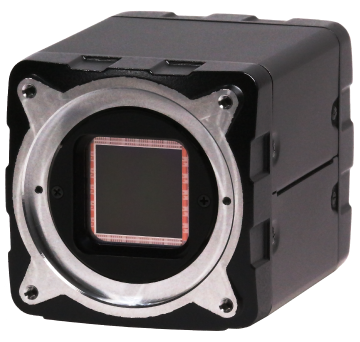
CoaXPress 2.0 Cameras
-
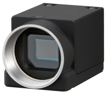
USB3 Cameras

-
GigE Cameras
-
Camera Link Cameras